Kyma Technologies, Inc., a leading supplier of ultra-high purity crystalline gallium nitride (GaN) and aluminum nitride (AlN) materials and related products and services, announced the addition of a new, denser form of ultra-high purity polycrystalline gallium nitride GaN targets to their PolyGaNTM product line.
|
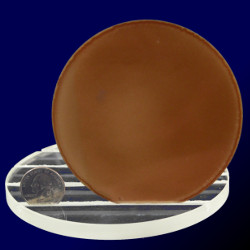
Kyma's PolyGaNTM products are manufactured using a proprietary process which leverages many of the features of Kyma's patent-protected native GaN boule growth process and are believed to be the highest purity polycrystalline GaN products available today. Kyma's PolyGaNTM Targets (see inset) have purity levels of 99.999% (5-nines) or higher (5-nines+) and are available in cylindrical disk form with diameters of 2", 3", and 4" at thicknesses that range from 2mm to 10mm. This new product is a lower surface area, denser, and higher purity form of PolyGaNTM in comparison to Kyma's PolyGaNTM Pellets (99.99% or 4-nines) which have been offered since 2005. Applications for Kyma's PolyGaNTM products include:
* Targets for plasma sputtering of III-nitride thin films
* Targets for pulsed laser deposition (PLD) of III-nitride device layers
* Feedstock for ammonothermal growth of bulk crystalline GaN
* Source material for sublimation growth of bulk crystalline GaN.
Dr. Ed Preble, Kyma's Chief Operating Officer, said, "Kyma's PolyGaNTM Targets represent a new standard in polycrystalline GaN in terms of purity, density, and low surface area, which provides benefits to our customers in terms of greater ease of handling and improved purity and control in their processes."
"Our original PolyGaNTM pellet products have already been successfully demonstrated in multiple processes by multiple customers," said Dr. Keith Evans, Kyma's president and CEO. "We believe these products to be the best available on the market today."
Special arrangements are possible, adds Evans: "We are flexible in the supply model. While or primary supply model is to be a direct supplier, we are open to strategic arrangements in which we can help our customers develop their own manufacturing capacity."
About Kyma Technologies
Kyma was launched in 1998 as a spin out of North Carolina State University's Materials Science and Engineering Department to pursue the development of gallium nitride (GaN) and aluminum nitride (AlN) substrates for a broad range of high performance nitride semiconductor device applications. Kyma's diversified product offering includes: ultra-low defect density native (free-standing) GaN in customer-defined orientation including polar (c-plane Ga-face or N-face) and non-polar (a-plane and m-plane), GaN and AlN templates grown on sapphire and other substrates, and ultra-high purity polycrystalline GaN. The market for nitride semiconductor devices is expected to surpass $9B by 2010. The combined addressable market for GaN and AlN substrates is expected to surpass $500M by 2010.
For more information about Kyma Technologies, please visit our website www.kymatech.com, send us e-mail at info@kymatech.com, or call the company directly at 919.789.8880.