Kyma Adds FLAAT GaN Templates to its Substrate Product Offering
Kyma Technologies, Inc., a leading supplier of advanced materials solutions that promote safety and energy efficiency, announced today the addition of FLAAT GaN templates to its substrate product offering.
The acronym FLAAT is short for Flat Layers At All Temperatures. FLAAT GaN templates consist of a layer of single-crystalline GaN grown by hydride vapor phase epitaxy (HVPE) on a sapphire substrate. Kyma employs a patented process for employing a stress balancing layer on the template backside to create a low-bow GaN template at all temperatures with an epi-ready surface finish.
Customers of this new product receive the benefits of a cost-effective low-defect density GaN buffer layer without the penalties of bow which accompany a simple template approach.
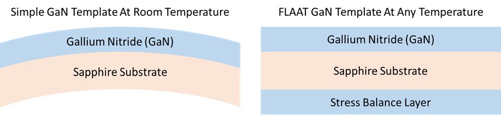
Above is a schematic diagram of a typical GaN on sapphire template (left) vs. FLAAT GaN template (right).
Kyma’s first FLAAT GaN template product is available in 2-inch diameter with 15 microns of crystalline GaN which is epi-ready with surface roughness RMS < 0.5 nm. Its wafer bow is <15 microns at all temperatures from room temperature up to typical metalorganic chemical vapor deposition (MOCVD) processing temperatures of 1100C.
Kyma’s FLAAT GaN template development activities have benefited from DOE SBIR support in a project led by Dr. Jacob Leach, who is Kyma’s Chief Science Officer, and monitored by Dr. Marina Sofos of the Department of Energy’s Advanced Manufacturing Office (AMO). That project recently transitioned to Phase II and is scheduled to be completed in early 2016.
The process for fabricating FLAAT GaN templates is scalable both in terms of substrate diameter and GaN layer thickness.
Today’s announcement is for the first of a series of FLAAT GaN products the company plans to produce. The next planned FLAAT GaN product offerings include a 50 micron thick 2-inch FLAAT GaN template as well as 4-inch and 6-inch diameter versions of the 15 micron thick product.
About Kyma Technologies
Kyma’s mission is to provide advanced materials solutions that promote safety and energy efficiency. Kyma’s products include a diverse portfolio of crystalline nitride semiconductor materials, crystal growth and fabrication equipment, and power switching electronics. Additionally, the company is developing a novel electromagnetic field sensor technology.
For more information about Kyma Technologies, visit www.kymatech.com, e-mail info@kymatech.com, or call the company directly at 919.789.8880.
Kyma is a registered trademark of Kyma Technologies, Inc.