Kyma Demonstrates High Quality 200-mm Diameter GaN on QST® Templates
Kyma Technologies, Inc., a leading developer of advanced wide bandgap semiconductor materials technologies, is pleased to announce it has used its new K200™ hydride vapor phase epitaxy (HVPE) growth tool to produce high quality 200-mm diameter HVPE GaN on QST® (QROMIS Substrate Technology) templates.
Today's announcement of Kyma's development of 200-mm diameter GaN on QST® templates follows its announcement in 2016 of its demonstration of 150-mm diameter GaN on QST® templates in partnership with QROMIS, Inc. (formerly Quora Technology, Inc.) and its recent announcement of the commissioning of Kyma's K200™ HVPE growth tool.
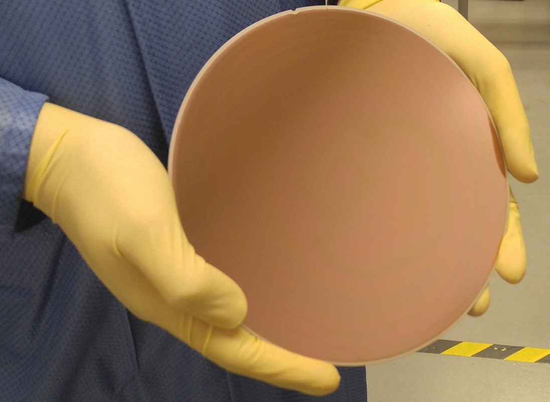
Pictured is one of the demonstrated 200-mm diameter HVPE GaN on QST® templates which consists of 10 microns of HVPE GaN grown on a 5 micron MOCVD GaN on QST® wafer provided by QROMIS, Inc. X-ray diffraction rocking curve linewidths for the templates fall in the range of 250 and 330 arc-sec for the symmetric {002) and asymmetric {102} XRD peaks, respectively, which is consistent with high structural quality. Low wafer bow (~50 microns) and smooth surface morphology suggest these materials should support high performance device manufacturing.
Kyma's newly constructed K200™ HVPE tool represents a first for the industry and was designed by Kyma engineers to enable uniform and rapid growth of high quality GaN on a number of different substrates.
Keith Evans, President & CEO, commented, "We have successfully transferred the process for making high quality GaN to our K200™ HVPE tool. The structural quality of the GaN produced on QROMIS’ QST® substrate is excellent. We are currently engaging with customers interested in large diameter GaN on QST® templates."
Kyma and Qromis are partnered for this work under a Kyma-led US DOE Phase IIB SBIR with award number DE-SC0009653.
QROMIS recently began manufacturing 200-mm QST® substrates and GaN-on-QST® wafers using its foundry partner Vanguard International Semiconductor (VIS). VIS is planning to offer GaN power device manufacturing services on 8-inch diameter QST® platform in 2018.
QROMIS co-founder & CEO Cem Basceri added, "QROMIS' CMOS fab-friendly 200-mm diameter QST® substrates and GaN-on-QST® wafers represent a disruptive technology, enabling GaN epitaxy from a few microns to hundreds of microns for GaN power applications from 100V to 1,500V or beyond GaN power devices, in lateral, quasi vertical or vertical forms, on the same 8-inch or 12-inch production platform at Si power device cost. Kyma's K200™ HVPE technology represents an important value-add to QST®-based GaN power device manufacturing by enabling the low cost deposition of a thicker and lower defect density GaN surface than is practically achievable using MOCVD growth alone."
Kyma is also teamed with a world-class semiconductor equipment OEM to manufacture K200™ HVPE tools for customers who prefer to bring Kyma's leading HVPE GaN growth process in-house.
About Kyma Technologies, Inc.
Kyma’s mission is to provide advanced materials solutions that promote energy efficiency. Kyma’s products include a diverse portfolio of advanced crystalline materials (including GaN, AlN, AlGaN, Ga2O3, and MoS2), crystal growth tools for fabricating such materials, and GaN-based photoconductive semiconductor switch (PCSS) devices. Kyma's growing service offering includes specialty parts manufacturing, device processing, materials characterization, wafer fabrication, and federal contract consulting services. For more information about Kyma, visit www.kymatech.com, send an email to info@kymatech.com, or call the company directly at +1 919.789.8880.
About QROMIS, Inc.
QROMIS, Inc., established in March 2015 as a spinoff from Micron Technology (Nasdaq: MU) and located in Silicon Valley, California, is a privately held fabless technology innovator focusing on energy efficient and high performance wide bandgap (WBG) semiconductor materials and device solutions which dramatically reduce global energy use and consumption.
The Company is poised to become one of the premier players in the rapidly growing, multi-billion dollar WBG industry with its disruptive and validated solutions in substrate and device technologies, which enable an unmatched cost, performance, and application scale. Markets served include power electronics, light emitting diodes (LEDs), advanced displays, and RF electronics, and other emerging high performance and energy efficient applications.
As a fabless company, QROMIS is driving the commercialization of its unique 8-inch diameter QST® substrates and GaN-on-QST® wafers with its foundry partner Vanguard International Semiconductor (VIS) (TWO : 5347). VIS offer 8-inch diameter GaN device foundry services on QST® platform, as well as access to advanced and novel process technology platforms, for the device customers. For more information about QROMIS, visit http://www.qromis.com.