Kyma Materials Help IEMN Scientists Reduce Leakage Currents in High-Voltage GaN-on-Si HEMTs
Kyma is pleased to be acknowledged for helping scientists at IEMN in France to realize high-voltage GaN-on-Si HEMTs with very low leakage currents.
IEMN (The Institute of Electronics, Microelectronics and Nanotechnology) recently published an open access journal article entitled "GaN-on-silicon high-electron-mobility transistor technology with ultra-low leakage up to 3000V using local substrate removal and AlN ultra-wide bandgap."
Additionally, a summary of that work entitled "High-voltage, ultra-low leakage HEMTs" was published in Compound Semiconductor Magazine in its April/May 2018 Volume (page 58).
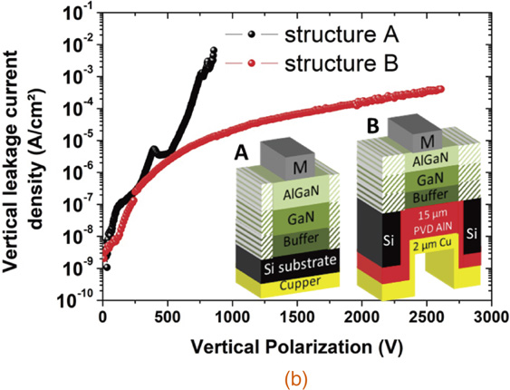
Those articles describe how IEMN researchers have now achieved GaN-on-Si HEMTs which exhibit a record combination of low leakage current and high blocking voltage. While IEMN had previously attained high standoff voltages of 3kV for GaN-on-Si HEMTs, they had suffered from high leakage currents of 1 mA/mm. The new 3kV devices reported on showed a 3-order of magnitude reduction in leakage current to less than 1 µA/mm which was enabled by thick AlN materials grown by Kyma within the backside trenches.
The figure shown above is a copy of Figure 3b from the Applied Physics Express article with caption "AlGaN/GaN epitaxial structures A and B, without and with LSR/backside AlN deposition, respectively."
The following are excerpts from the Compound Semiconductor Magazine article:
"Front-side processing followed, involving: the addition of Ti/Al/Ni/Au ohmic contacts, directly on the AlGaN barrier; device isolation by nitrogen implantation; deposition of a Ni/Au stack on the SiN cap to create metal-insulator-semiconductor structures; and a further deposition of 200 nm of SiN to provide additional passivation. To complete fabrication, the engineers locally etched the substrate up to the AlN nucleation layer, so that silicon is removed up to 50 μm away from the sidewalls, before adding a 15 μm-thick layer of AlN.
The latter step is undertaken by Kyma Technologies. “They had already experience with thick PVD deposition of high resistive AlN,” explains Medjdoub, “and deposition in their case can be performed on large wafer diameters.”
Kyma's CEO Dr. Keith Evans commented, "We are pleased to assist IEMN researchers in the advancement of their device performances. We believe their results speak well to the excellent capabilities Kyma has developed over the years in advanced plasma vapor deposition technology."
About IEMN (The Institute of Electronics, Microelectronics and Nanotechnology)
The Institute of Electronics, Microelectronics and Nanotechnology or IEMN is a research institute of the Université Lille Nord de France. For more information about IEMN visit https://www.iemn.fr/en/.
About Kyma Technologies, Inc.
Kyma’s mission is to provide advanced materials solutions that promote energy efficiency. Kyma’s products include a diverse portfolio of advanced crystalline materials (including GaN, AlN, AlGaN, Ga2O3, and graphene), crystal growth tools for fabricating such materials, and GaN-based photoconductive semiconductor switch (PCSS) devices. Kyma's growing service offering includes specialty parts manufacturing, device processing, materials characterization, wafer fabrication, and federal contract consulting services.
To access scientific publications which feature Kyma's technologies, click here.
For more information about Kyma, visit www.kymatech.com, send an email to info@kymatech.com, or call the company directly at +1 919.789.8880.