Materials Characterization
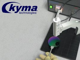
Kyma customers benefit from Kyma's in-house suite of routine characterization tools and its quick access to local advanced characterization facilities.
Kyma also has rapid access to a number of advanced characterization tool at partner facilities in The Triangle for which Kyma staff is trained and certified to use. Kyma also has long standing relationships with a number of outsource characterization service providers and we can put together a characterization proposal that fits you needs based on an optimized combination of in-house, local, and outsource capabilities.
Kyma's routine in-house characterization capabilities include:
| Electrical Resistivity: | High-resistivity measurement of semi-insulating semiconductor bulk substrates and other materials ranging from 5x10⁴ to 5x10⁹ Ohm-cm with sizes from 10mm x 10mm squares to 150mm diameter and thicknesses between 350 and 650um |
| Low to medium resistivity sheet resistance, resistivity and thickness of semiconductor bulk substrates and thin films ranging from 0.035 to 3000 Ohms/square with sizes from 5mm x 5mm squares to 100mm in diameter. | |
| Surface Morphology: | White light interferometric surface morphology mapping of thin and thick film substrates. Dimensions capability includes 1mm x 1mm to 4 inches in diameter. |
| Thickness: | Contactless measurements of semiconductor thin films ranging from 150Å to 450µm with sizes from 5mm x 5mm squares to 100mm in diameter. |
| Thickness & Bow: | Contactless single-probe, multi-point thickness mapping and bow measurement of thin and thick films on substrates up to 4 inches in diameter. |
| X-Ray Diffraction: | A number of different XRD measurements are possible, from simple rocking curves and theta-2 theta curves to full reciprocal space maps. We can also simulate XRD spectra and compare with measured spectra. |
Kyma's external characterization capabilities include: AFM, SIMS, Raman Spectroscopy, SEM, TEM, High Resolution X-ray Computed Tomography, UV-VIS-NIR Spectroscopy, FTIR Spectrometry, and Photoluminescence.